03. July 2014 | Press releases
Chinese semiconductor specialist Enkris Semiconductor, Inc. has successfully demonstrated the manufacture of high voltage Gallium Nitride HEMT (High Electron Mobility Transistor) structures on 200 mm Silicon (GaN-on-Si) with an AIXTRON tool.
GaN-on-Si power devices have attracted much attention from both academics and industry recently because of their potential applications in power electronics. Due to the defective nature of heteroepitaxial GaN layers grown on silicon, GaN-on-Si power devices have suffered from high buffer leakage. Most recently, Enkris Semiconductor has produced high voltage GaN HEMT materials on 200 mm silicon with excellent uniformity and low buffer leakage combined with excellent thickness uniformity of below 0,5 percent without edge exclusion. Under special conditions the uniformity value can be improved even further.
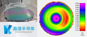
Figure 1: Thickness mapping of 200 mm GaN-on-Si wafers
“It has been well accepted that GaN on large size silicon substrates is the most cost-effective way to achieve high-volume production of GaN power devices. However, a large wafer bow combined with a high buffer leakage has hindered the further development of the GaN-on-Si technology so far. Our process on 200 mm silicon substrates shows that high breakdown voltage (less than 1600 V) GaN power devices with low leakage currently can be achieved with relatively thin buffer layers of 4 µm. They simplify the growth process, minimize the wafer bow and reduce the epi-cost significantly. Based on our processes which were applied on an AIXTRON system, GaN-on-Si power devices may reach even higher voltages in the near future,” comments Dr. Cheng Kai, co-founder of Enkris.
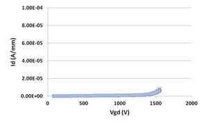
Figure 2: Current leakage of devices fabricated on 200 mm GaN-on-Si wafers.
Dr. Frank Wischmeyer, Vice President Power Electronics at AIXTRON, says: “Enkris‘ remarkable success in achieving excellent layer quality and material properties show the capability of our technology for high-voltage GaN HEMT applications. Our MOCVD technology is enabling the integration of wide-bandgap semiconductors on large diameter silicon substrates. AIXTRON is committed to support the power electronics industry advancing toward high volume 200 mm GaN-on-Si device manufacturing.”
Our registered trademarks: AIXACT®, AIXTRON®, Atomic Level Solutions®, Close Coupled Showerhead®, CRIUS®, EXP®, EPISON®, Gas Foil Rotation®, Optacap™, OVPD®, Planetary Reactor®, PVPD®, STExS®, Trijet®
Christian Ludwig
Vice President Investor Relations & Corporate Communications
Alan Tai
Taiwan/Singapore
Christof Sommerhalter
USA
Christian Geng
Europe
Hisatoshi Hagiwara
Japan
Nam Kyu Lee
South Korea
Wei (William) Song
China
AIXTRON SE (Headquarters)
AIXTRON 24/7 Technical Support Line
AIXTRON Europe
AIXTRON Ltd (UK)
AIXTRON K.K. (Japan)
AIXTRON Korea Co., Ltd.
AIXTRON Taiwan Co., Ltd. (Main Office)
AIXTRON Inc. (USA)
Christoph Pütz
Senior Manager ESG & Sustainability
Christian Ludwig
Vice President Investor Relations & Corporate Communications
Ralf Penner
Senior IR Manager
Christian Ludwig
Vice President Investor Relations & Corporate Communications
Prof. Dr. Michael Heuken
Vice President Advanced Technologies