18. April 2016 | Compound Semiconductors
AIXTRON’s production technology integrates imec’s proprietary materials technology to increase performance of GaN-on-Si-based power devices

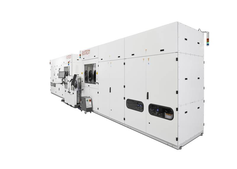
AIXTRON SE (FSE: AIXA; NASDAQ: AIXG), a worldwide leading provider of deposition equipment to the semiconductor industry, announced today that its G5+ C multi-wafer batch MOCVD platform has been qualified for the manufacturing of specific buffer layers as a result of the collaboration on high-voltage gallium nitride (GaN) power device technology with Belgian nanoelectronics research center imec (Interuniversity Microelectronics Centre).
Most recently, both AIXTRON and imec received the prestigious 2016 CS Industry Award in the categories of “High Volume Manufacturing” for AIXTRON’s G5+ C and “Substrates and Materials” for imec’s GaN-on-Si materials development. In combining their expertise, AIXTRON has joined imec’s industrial affiliation program for high power GaN-on-Si device technology. Within the framework of this program, AIXTRON’s 5x200 mm G5+ MOCVD platform was qualified to integrate imec’s proprietary high-voltage dispersion free buffer technology to the 5x200 mm G5+ MOCVD platform. This goal has been reached in a very short time span and demonstrates the high level of technology readiness of the AIX G5+ C system.
Dr. Frank Wischmeyer, Vice President Marketing and Business Development Power Electronics at AIXTRON, comments: “We are delighted to announce the successful qualification of imec’s proprietary 200 mm GaN-on-Si materials technology on our G5+ C high-volume manufacturing platform. The accomplishment was mainly based on the rapid implementation of the portfolio of qualified layer processes by the epitaxy teams of imec and AIXTRON building up the complex epitaxial material stack targeting high voltage switching applications.”
"imec targets high-performing and reliable GaN power devices requiring a concerted effort between device and material engineering“, says Rudi Cartuyvels, Senior Vice President Smart Systems and Energy Technologies at imec. “As the AIX G5+ C enables exactly this, we are pleased with the fast transfer of our device structure processes onto the new platform. We are happy that AIXTRON is part of imec’s GaN industrial affiliation program and look forward to a continuation of the successful collaboration”.
AIXTRON’s G5+ C is the first fully automated GaN-on-Si production system including a cassette-to-cassette wafer loading system and automated reactor in-situ clean. At the same time, the Planetary batch AIX G5+ C system demonstrated highest uniformity control of layer properties and lowest particle.
Based on a portfolio of qualified MOCVD processes at AIXTRON, tailored for the needs of the GaN-on-Si power HEMT industry, typical challenges like strain engineering of the AlGaN/GaN material on 200 mm Si substrates, high quality AlN nucleation on Si substrates and the pit free growth of high quality buffer layers could be addressed successfully in the cooperation with imec.
Our registered trademarks: AIXACT®, AIXTRON®, Atomic Level Solutions®, Close Coupled Showerhead®, CRIUS®, EXP®, EPISON®, Gas Foil Rotation®, Optacap™, OVPD®, Planetary Reactor®, PVPD®, STExS®, Trijet®

Christian Ludwig
Vice President Investor Relations & Corporate Communications
Alan Tai
Taiwan/Singapore
Christof Sommerhalter
USA
Christian Geng
Europe
Hisatoshi Hagiwara
Japan
Nam Kyu Lee
South Korea
Wei (William) Song
China
AIXTRON SE (Headquarters)
AIXTRON 24/7 Technical Support Line
AIXTRON Europe
AIXTRON Ltd (UK)
AIXTRON K.K. (Japan)
AIXTRON Korea Co., Ltd.
AIXTRON Taiwan Co., Ltd. (Main Office)
AIXTRON Inc. (USA)
Christoph Pütz
Senior Manager ESG & Sustainability
Christian Ludwig
Vice President Investor Relations & Corporate Communications
Ralf Penner
Senior IR Manager
Christian Ludwig
Vice President Investor Relations & Corporate Communications
Prof. Dr. Michael Heuken
Vice President Advanced Technologies