Deposition Systems for Compound Semiconductors

G10-GaN

150/200 mm high throughput epitaxy

for GaN power & RF applications 

.

Our product for 150/200 mm GaN epitaxy

G10-GaN 

  • Highest wafer/m² fab area
    3 process chamber compact cluster design with
    50 % footprint reduction*


  • Best in class device yield

3x on-wafer uniformity improvement*
at lowest particle level for all wafers
(within run, run-to-run, chamber-to-chamber)
 

  • Lowest epi cost/wafer in the market

>25% lower epi cost than any other platform 

Planetary Reactor® 

Your benefits 

  • Highest wafer yield
    Low particle density (~0.1/cm²)
    Excellent uniformity (on-wafer, wafer-to-wafer)


  • Best in class productivity
    Outstanding reproducibility
    ≥90 % equipment uptime
  • Best in class epi cost
    Highest throughput/m² fab
    Lowest labor & chemical cost 

Our solutions

  • Fully automated wafer handling (C2C)
  • Novel wafer carrier design
  • Individual wafer close loop topside temp. control
  • Individual control of thickness & composition uniformity by 5-flow injector
  • Automated chamber cleaning
  • Long lifetime consumables
  • Smart system with predictive functionalities
  • Advanced chamber-to-chamber matching capabilities
  • Large capacity batch Planetary Reactor®
  • Compact cluster design with 3 process chambers
  • Highest chemical efficiency by 5-flow injector
  • Lowest operator assistance due to 50 wafer capacity on C2C 

The best of both worlds

Single wafer performance at lowest batch processing cost 


Composition uniformity 

On-wafer device uniformity (650V application) 

G10-GaN enables seamless process transfer from today‘s tool of record AIX G5+ C

  • Same cassette-to-cassette wafer handling


  • „On-board“ calibration and control modes for process matching


  • Identical process chamber size and wafer configuration 

High productivity MOCVD solution for 150/200 mm GaN power & RF applications

Market opportunity

GAN MARKET TRENDS


FAST CHARGER

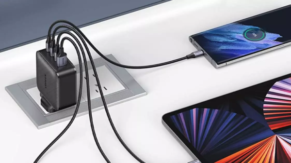
Source: https://www.digitalcameraworld.com/buying-guides/best-gan-charger


DATA CENTER

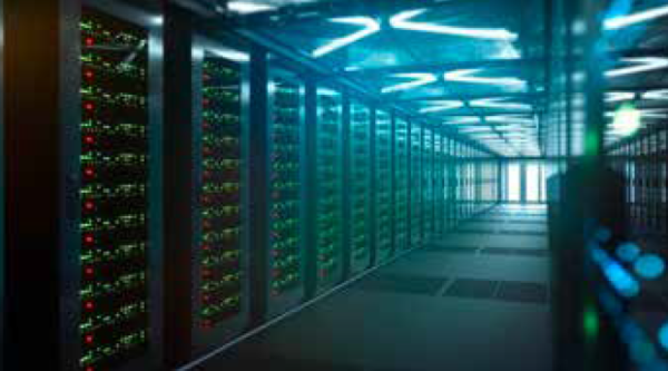
Source: https://www.datacenterknowledge.com


SOLAR MICRO INVERTER

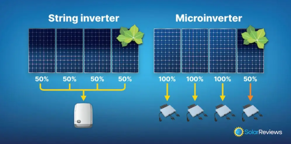
Source: https://www.solarreviews.com 

Market volume ($M)

Source: Yole Power GaN © 2023 

Global presence 

CHINA
AIXTRON China Ltd.
Phone +86 (21) 6445 3226
Fax +86 (21) 6445 3742
E-Mail chinainfo@aixtron.com

GERMANY
AIXTRON SE
Phone +49 (2407) 9030-0
Fax +49 (2407) 9030-40
E-Mail info@aixtron.com

TAIWAN
AIXTRON Taiwan Co., Ltd.
Phone +886 (3) 571 2678
Fax +886 (3) 571 2738
E-Mail taiwaninfo@aixtron.com

KOREA
AIXTRON Korea CO., Ltd.
Phone +82 (31) 371 3000
Fax +82 (31) 371 3093
E-Mail koreainfo@aixtron.com

USA
AIXTRON Inc.
Phone +1 (669) 228 3759
E-Mail usinfo@aixtron.com

UNITED KINGDOM
AIXTRON Ltd.
Phone +44 (1223) 519 444
Fax +44 (1223) 519 888
E-Mail ukinfo@aixtron.com

JAPAN
AIXTRON K.K.
Phone +81 (3) 5781 0931
Fax +81 (3) 5781 0940
E-Mail japaninfo@aixtron.com

MALAYSIA
AIXTRON Malaysia Sdn. Bhd.
E-Mail info@aixtron.com


DOWNLOAD BROCHURE 


Brochure-G10-GaN.pdf

Service

AIXTRON SE (Headquarters)

AIXTRON 24/7 Technical Support Line

AIXTRON Europe

AIXTRON Ltd (UK)

AIXTRON K.K. (Japan)

AIXTRON Korea Co., Ltd.

AIXTRON Taiwan Co., Ltd. (Main Office)

AIXTRON Inc. (USA)

Produkte

Vincent Meric
Vice President Marketing

Karriere

Laura Preinich
Recruiter

Tom Lankes
Talent Acquisition Expert - Ausbildungsleitung

Nachhaltigkeit 

Christoph Pütz
Senior Manager ESG & Sustainability

Unternehmen & Investor Relations

Carsten Werle
Director Investor Relations (Interim)

Forschung & Entwicklung

Prof. Dr. Michael Heuken
Vice President Advanced Technologies

Presse & Öffentlichkeitsarbeit

Ragah Dorenkamp
Director Corporate Communications